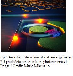
Photons and electrons are the basic particles playing a major role towards designing and working of most of the technical devices. Scientists and engineers are always looking for new ways to manipulate and control the behavior of electrons and photons in order to produce the desired effects in general and electricity in particular. Optoelectronics, the devices that detect, create, and manipulate various forms of light from visible light to X-rays, gamma rays, infrared, and ultraviolet light, are already in use for military services, telecommunications, automatic access control systems and in medical equipment. Putting a low-dimensional material under strain can change the values of all the material parameters. This means there’s the possibility of designing materials according to our needs for all kind of applications by applying strain only on the material. In this direction, researchers recently have found a new way to engineer optoelectronic devices with improved characteristics by applying strain through stretching a two-dimensional material on top of a silicon photonic platform. Using this method, coined strainoptronics by a team led by Prof. Volker Sorger of George Washington University (USA), the researchers demonstrated for the first time that a 2D material wrapped around a nanoscale silicon photonic waveguide creates a novel photodetector making it able to operate with high efficiency at the technology-critical wavelength of 1550 nanometers. Such new photodetection can advance future communications and computer systems, especially in emerging areas such as machine learning and artificial neural networks.
Strain application to manipulate materials properties by altering its mechanical or structural attributes has been a top agenda for scientists and engineers and the field is termed as strain engineering. Thin two-dimensional nano materials (2DNMs) are particularly well-suited for strain engineering because they can withstand large strain as compared to bulk materials. Different methods/techniques like: thermal vibration, surface adhesion, substrate deformation, pre-stretched substrate, epitaxial grown, thermal expansion mismatch, substrate topography modification, pressurized blisters and tip indentation can result in strain generation. Application of strain in thin two-dimensional nano materials can modify their atomic structure, lattice vibration, thermal conductivity, electronic and optical, electrical and device performance, and chemical activities. Through applying uniform deformation, or via localised structures, strain engineering in two-dimensional materials allows for the control or enhancement of their unique properties, which may yield numerous benefits for applications in future.
The ever-increasing data demand of modern societies requires a more efficient conversion of data signals in the optical domain, from fiber optic internet to electronic devices, like a smartphone or laptop. This conversion process from optical to electrical signals is performed by a photodetector, a critical building block in optical networks. However, 2-D semiconducting materials such as those from the family of transition metal dichalcogenides because of their large optical band gap and low absorption have, so far, not been able to operate efficiently at telecommunication wavelengths. Strainoptronics can provide a solution to this shortcoming and adds an engineering tool for researchers to modify the electrical and optical properties of 2-D materials. Thin two dimensional materials because of their strong optical absorption have scientific and technologically relevant properties for photodetectors. Thus, designing a 2-D material-based photodetector would enable an improved photo-conversion, and hence more efficient data transmission and telecommunications.
By realizing the potential of strainoptronics in recent developments, the researchers by stretching an ultrathin layer of molybdenum telluride (2-D material semiconductor) on top of a silicon photonic waveguide could assemble a novel photodetector. They then used the newly created strainoptronics “control knob” to alter its physical properties to minimize the electronic band gap, allowing the device to operate at near infrared wavelengths (namely at the telecommunication (C-band) relevant wavelength around 1550 nm). The researchers noted one interesting aspect of their discovery that the amount of strain these semiconductor 2-D materials can bear is significantly higher when compared to bulk materials for a given amount of strain. They also note these novel 2-D material-based photodetectors are 1,000 times more sensitive compared to other photodetectors using graphene. Photodetectors capable of such extreme sensitivity are useful not only for data communication applications but also for medical sensing and possibly even quantum information systems. The researchers mentioned that they have not only found a new way to engineer a photodetector, but also discovered a novel design methodology for optoelectronic devices. Interestingly, unlike bulk materials, two-dimensional materials are particularly promising candidates for strain engineering because they can withstand larger amounts of strain before rupture. In the near future, they want to apply strain dynamically to many other two-dimensional materials in the hopes of finding endless possibilities to optimize photonic devices.
Acknowledgement: The use of information retrieved through various references/sources of internet in this article is highly acknowledged.


